

D06: BITS TO WAVES AND BACK - PROJECT REPORT
Abstract
Abstract
NATIONAL INSTITUTE OF TECHNOLOGY KARNATAKA, SURATHKAL
D06: BITS TO WAVES AND BACK - PROJECT REPORT
SUBMITTED BY :
Aditya S 241EC2
Ishaan Bharadwaj 241EC
Rhea Mishra 241EC
Sinchana R 241EC253
Under the guidance of
Aditya Santhanam
Prateek Goel
Shreyan Ghosh
Submitted on: 22nd May 2025
GOOGLE MEET LINK: https://meet.google.com/jas-cddv-azb
Aim of the project
This project aims to understand the working principles, types, and applications of Digital to Analog Converters (DACs), which play a key role in modern electronic systems. By studying different DAC architectures—such as Binary Weighted, R-2R Ladder, Current Switching, and Current Steering—the project seeks to analyze how digital signals are accurately converted into analog outputs. The objective also includes comparing the strengths and limitations of voltage-mode and current-mode DACs in terms of speed, linearity, resolution, and power efficiency. This knowledge forms the foundation for designing and implementing efficient data conversion systems in real-world applications like audio processing, communication systems, and embedded devices.
INTRODUCTION:
To begin with, digital signals are the language of all computers systems and only take the binary values 0 and 1. While all processes related to the environment and the natural world are represented in the form of analog signals, which are arbitrary time signals. Most often, a conversion between analog to digital is desired or vice-versa. This is where the study of analog to digital converters and digital to analog converters comes into play. Lets have a quick overview of analog and digital signals.
Analog Signal:
An analog signal is a type of signal that represents continuous data using a continuous range of values. It varies smoothly over time and can take any value within a given range. For example, a sound wave in its natural form is an analog signal, where the electrical signal continuously mirrors the fluctuations in air pressure.
Digital Signal:
A digital signal represents data using a sequence of discrete values, usually in binary (0s and 1s). Unlike analog signals, digital signals are not continuous; they are quantized and take on specific voltage levels. Digital signals are widely used in computing, telecommunications, and multimedia systems due to their efficiency in processing, transmission, and storage.
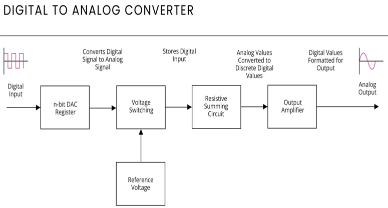
Digital to Analog Converter (DAC):
A digital to analog converter (DAC) is a circuit that transforms a digital signal, typically a sequence of 1s and 0s, into an analog signal, which can be a voltage or current. Few examples include Audio Systems; DACs play a crucial role in audio systems, converting digital audio data into analog signals. Signal generators and Data Acquisition Systems are some other applications.
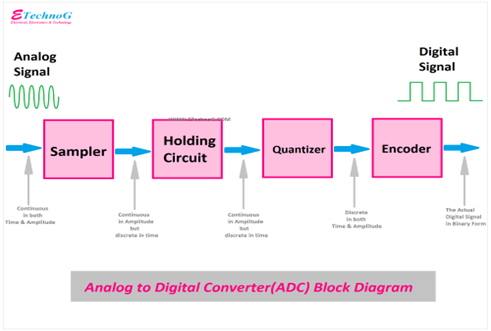
Analog to Digital converters (ADCs):
These convert continuous real time signals into digital signals which computing systems can understand. First, the analog signal is sampled at the Nyquist rate (Sampling frequency is twice the maximum available frequency). Then, after sampling, the signal’s amplitude is quantised, converting the continuous stream of amplitude values into discrete values. Finally, the signal is passed through an encoder and the final output is generated.Some examples of ADCs are the following; Function generators, Motor control systems, audio playback and many more.
Voltage based DACs:
Types of DACs:
Binary weighted Resistance DAC
Consider a 4 bit Binary weighted resistance DAC as shown below:
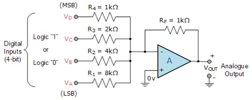
VA corresponds to Least significant bit in the digital input whereas VD corresponds to most significant bit in the digital input.
On roughly analysing we understand that this is an inverting-summing amplifier
In general the Output voltage of an inverting summing amplifier is given by
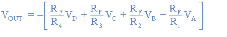
In this case , the formula modifies into
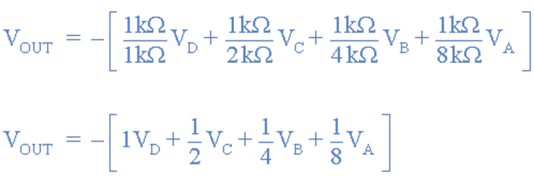
For a 4-bit binary number there are 2^4 = 16 possible combinations or A, B, C, and D ranging from 0000 to 1111 which corresponds to decimal 0 to 15 respectively. If we assign weights to each input bit such that each bit has double the weight of the previous bit , it will create binary codes with weight 8,4,2,1. Weights here can be physically interpreted with the value of resistances.
Thus according to this if we consider D input resistance as 1k ohms then C would be 2k ohms similarly B and A would ve 4k and 8k ohms respectively. Feedback resistance is 1k ohm.
Consider Vin = V. If input at terminal D is high( logic 1) ie V is applied at this terminal (ie MSB) , with other inputs being low (thus LSB = 0) . Calculating Vout from the above mentioned formula
Vout = -[1/1 * Vd +0+0+0] = -Vd .Thus output voltage is -V, when input is 1000 in binary form
Consider Vin = V. If input at terminal C is high( logic 1) ie V is applied at this terminal , with other inputs being low . Calculating Vout from the above mentioned formula
Vout = -[0 +½ * Vc+0+0] = -Vc/2 .Thus output voltage is -V/2 , when input is 0100 in binary form.
Consider Vin = V. If input at terminal B is high( logic 1) ie V is applied at this terminal , with other inputs being low. Calculating Vout from the above mentioned formula
Vout = -[0+0+¼*Vb+0] = -Vb/4 .Thus output voltage is -V/4, when input is 0010 in binary form.
Consider Vin = V. If input at terminal A is high( logic 1) ie V is applied at this terminal (ie LSB) , with other inputs being low (thus MSB = 0) . Calculating Vout from the above mentioned formula
Vout = -[0+0+0+⅛*Va] = -Va/8 .Thus output voltage is -V/8, when input is 0001 in binary form.
With such sorts of permutation, calculating Vout for all digital inputs from 0000 to 1111, we get the outputs as tabulated below:
Digital Inputs (D C B A)
VOUT Expression
VOUT (in terms of V)
0 0 0 0
"0*V + 1/2*0*V + 1/4*0*V + 1/8*0*V"
"0"
0 0 0 1
"0*V + 1/2*0*V + 1/4*0*V + 1/8*1*V"
"-0.125 * V"
0 0 1 0
"0*V + 1/2*0*V + 1/4*1*V + 1/8*0*V"
"-0.250 * V"
0 0 1 1
"0*V + 1/2*0*V + 1/4*1*V + 1/8*1*V"
"-0.375 * V"
0 1 0 0
"0*V + 1/2*1*V + 1/4*0*V + 1/8*0*V"
"-0.500 * V"
0 1 0 1
"0*V + 1/2*1*V + 1/4*0*V + 1/8*1*V"
"-0.625 * V"
0 1 1 0
"0*V + 1/2*1*V + 1/4*1*V + 1/8*0*V"
"-0.750 * V"
0 1 1 1
"0*V + 1/2*1*V + 1/4*1*V + 1/8*1*V"
"-0.875 * V"
1 0 0 0
"1*V + 1/2*0*V + 1/4*0*V + 1/8*0*V"
"-1.000 * V"
1 0 0 1
"1*V + 1/2*0*V + 1/4*0*V + 1/8*1*V"
"-1.125 * V"
1 0 1 0
"1*V + 1/2*0*V + 1/4*1*V + 1/8*0*V"
"-1.250 * V"
1 0 1 1
"1*V + 1/2*0*V + 1/4*1*V + 1/8*1*V"
"-1.375 * V"
1 1 0 0
"1*V + 1/2*1*V + 1/4*0*V + 1/8*0*V"
"-1.500 * V"
1 1 0 1
"1*V + 1/2*1*V + 1/4*0*V + 1/8*1*V"
"-1.625 * V"
1 1 1 0
"1*V + 1/2*1*V + 1/4*1*V + 1/8*0*V"
"-1.750 * V"
1 1 1 1
"1*V + 1/2*1*V + 1/4*1*V + 1/8*1*V"
"-1.875 * V"
By increasing the number of binary digits and the resistive summing network so that each resistor has a different weighting, the resolution of the analogue output voltage for a binary weighted digital-to-analogue converter can be increased.
Advantages of Binary Weighted Resistor DAC:
Simple design and easy to implement due to its straightforward architecture.
Offers good linearity and accuracy if resistor values are well matched.
Provides fast digital-to-analog conversion.
Supports higher resolution and a wide range of analog outputs.
Consumes less power compared to other DAC types.
Disadvantages of Binary Weighted Resistor DAC:
Difficult and expensive to implement at higher bit resolutions.
Requires very precise resistor values, which are hard to maintain.
Power consumption increases with more bits.
Accuracy drops due to physical limitations and mismatch at high resolutions.
May face issues like switching errors and longer settling time.
2. R-2R Ladder DAC
Consider a 4 bit R-2R DAC as shown below:
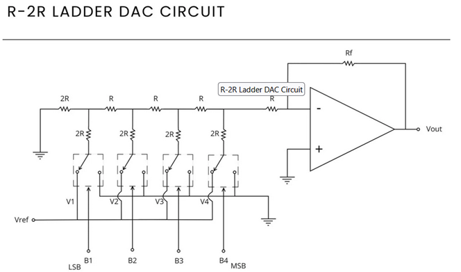
A 4-bit digital input is applied to the DAC.Each bit corresponds to a specific voltage level determined by its position in the ladder.This DAC consists of a combination of resistors with values R and 2R.Each bit of the digital input is connected to a switch. If the bit is a "1", the corresponding switch connects the point in the ladder to Vref. If the bit is a "0", the switch connects it to ground.The ladder network acts as a voltage divider. The output voltage is the weighted sum of the voltages at each point in the ladder.
Example:
If the input is 1011:
Bit 3 (MSB) is 1: Connect the corresponding point to Vref. This contributes Vref to the output.
Bit 2 is 0: Connect the corresponding point to ground. This contributes 0 to the output. Bit 1 is 1: Connect the corresponding point to Vref. This contributes Vref/2 to the output. Bit 0 (LSB) is 1: Connect the corresponding point to Vref. This contributes Vref/4 to the output.
The output voltage(Vout) is the sum of the contributions from each bit: Vout=Vref+0+Vref/2+Vref/4.
R-2R Ladder DAC uses a resistor network to divide the reference voltage and switch between Vref and ground based on the digital input bits, creating an analog output voltage that corresponds to digital input.
Disadvantages of R-2R Ladder DAC:
One of the significant disadvantages of R-2R Ladder DAC is its limited resolution and accuracy. The resolution of an R-2R Ladder DAC is determined by the number of resistors in the ladder network. The more resistors used, the higher the resolution, but this also increases the complexity and cost of the DAC. The main reason for this limitation is the mismatch between the resistors in the ladder network. Even with careful selection and matching of resistors, small variations in their values can lead to significant errors in the output voltage. This affects the accuracy of the DAC, resulting in a lower signal-to-noise ratio (SNR) and increased distortion.
Switching to a current-based architecture for DACs:
This design relies upon using matched current sources and switches, wherein a current is produced as an output and then converted into voltage later in the circuit. (The most basic one involves manual switching)
But Why make the switch to a current-based architecture?
There are some major advantages that this design possesses over the former and are described in detail below.
Higher speed: Current-mode DACs can operate at higher switching speeds because they avoid the charging and discharging of capacitive loads inherent in voltage-mode DACs.
Better linearity: Their overall deviation from the ideal step-size and ideal transfer characteristics is less than for a voltage based architecture and therefore achieve more accurate results.
Scalability: They can easily be scaled to inputs with more than 10+ bits as they can be matched precisely with silicon while voltage based architectures can become much more difficult to handle beyond this threshold.
Power efficiency: Due to the avoidance of parasitic capacitance in this design, the consumption of power is less, and hence can operate with lower input power.
CMOS integration: This technology naturally lends itself to current-mode circuits due to the ease of implementation of current mirrors and current sources.
Voltage-mode DACs, however, often require precision resistors or capacitors, which are harder to match and more area-consuming in CMOS and thus make them more difficult to use in miniaturized electronic circuits such as ICs(integrated circuits).
Therefore, given all these factors, in modern times, most often current-based architectures are at the heart of all major electronic circuitry.
Current Switching DACs:
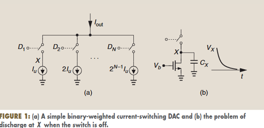
This circuit is an example of simple binary-weighted DAC. We can call it a current switching.
BASIC TOPOLOGY
Now we wish to convert an N-bit digital signal, Din ,to an analog current I out.This can be accomplished as shown in figure1(a).where each input bit controls a current that is binarily
weighted with respect to a unit value,Iu.Now here D1 denotes the least significant bit(LSB) and Dn the most significant bit (MSB). Here the current sources are scaled up by a factor of two from one bit to the next,yielding
![]()
The advantage of this DAC is that it has the ability to drive loads with no need of a buffer. This property proves crucial if the DAC must drive a trans-mission line, as in wireline systems,or if the load contains a resistive component, as in displays and opti-cal modulators.
The current-switching structure shown in Figure 1(a) suffers from dynamic errors. As depicted in Figure 1(b), when a switch turns off, the top terminal voltage of its corresponding current source collapses to zero. Thus, the next time that this branch is enabled, the (nonlinear) capacitance at this terminal must charge up, drawing a significant transient current from the output node. Moreover, since switching actions change the total current carried by the array, the ground voltage experiences large fluctuations in the presence of parasitic series inductances, such as those due to bond wires. Both of these effects can be greatly suppressed through the use of current steering.
Disadvantages of Current Switching DACs:
These have several drawbacks too, including output transients (glitches), complex design, and potential for noise. They also require decoding schemes to mitigate glitches and can have dynamic performance limitations mostly for higher-resolution DACs. Designing and implementing current-switching DACs can be challenging, requiring careful consideration of factors like switch matching, current source accuracy, and layout.
Current Steering DAC:
There is a switch made to the current-steering design for DACs from current-switching DACs. This is because the issue of parasitic inductances and capacitances are sorted by the use of an additional MOSFET which mirrors exactly the same current as in the original and hence greatly speeds up the process of producing the output current.
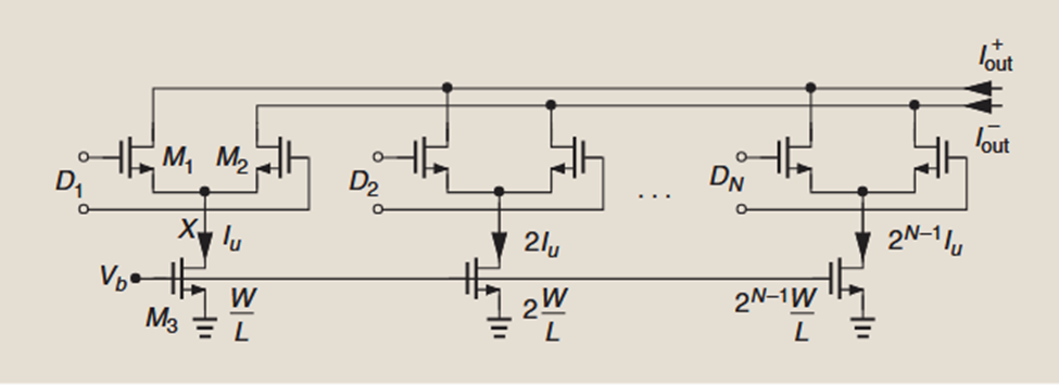
This is a figure of binary-weighted current steering DAC.Now here, the tail current is steered to the left or the right by each differential pair, causing only a small voltage excursion at node X. Now , since the total array current is relatively constant, the ground bounce is much smaller. Of course, another advantage of this configuration is that it naturally provides differential outputs.
Working of current steering DAC:
1. The DAC utilizes an array of current sources, each with a specific current value .These current sources are connected to switches, which are controlled by the digital input code.
2. Now when a digital input is applied, the switches open or close, directing the current from the selected current sources to the output node. The combination of currents flowing through the switches determines the final output current, which is then converted to an analog voltage by a load resistor.
3. These current sources can be weighted in a binary fashion (like 1I, 2I, 4I, 8I, etc.) or other schemes, depending on the DAC architecture. This allows for a wider range of analog output values.
4. The summed current is then passed through a load resistor, creating a voltage output proportional to the digital input code. This voltage represents the analog representation of the digital input.

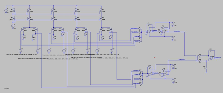
This table demonstrates the difference between the output voltages produced by the current switching and current steering DACs. In diff voltage (V), the issue of noise is eradicated, as both the inverting op-amps produce the same amount of error due to the environment, so both errors then get inputted in the subtractor and hence add up to zero in the end. Then also the issue of common mode error gets eliminated as margin between voltages increases to 1 which is comparable to the increase between the binary values, so the error is now less significant. The circuit implementation of this is shown below:
Conclusion: This project gave a clear understanding of how DACs convert digital signals into analog form using different architectures like binary-weighted, R-2R ladder, and current-mode DACs. We saw how each method has its own use — voltage-based DACs are simple, while current-mode DACs are faster and more accurate. In modern circuits, current steering DACs are widely used because they handle speed, power, and noise better. Overall, this helped us learn how important DACs are in bridging the digital-analog gap in real-world electronics.
Bibliography:
www.rfwireless-world.com
https://nerdsdostuff.com/electronic_circuits/digital-to-analog-converter-dac-basics-and-workig/
https://www.electronics-tutorials.ws/combination/digital-to-analogue-converter.html
https://microcontrollerslab.com/binary-weighted-resistor-dac-working-example-circuits-advantages/
https://www.tek.com/en/blog/tutorial-digital-analog-conversion-r-2r-dac?bpv=2
https://www.analog.com/en/resources/design-notes/applications-of-current-dacs.html
https://www.seas.ucla.edu/brweb/papers/Journals/BRWinter18DAC.pdf
Report Information
Team Members
Team Members
Report Details
Created: May 23, 2025, 2:21 a.m.
Approved by: Gururaj Shimpi [Diode]
Approval date: May 25, 2025, noon
Report Details
Created: May 23, 2025, 2:21 a.m.
Approved by: Gururaj Shimpi [Diode]
Approval date: May 25, 2025, noon